Information regarding the chemical composition, physical properties, and three-dimensional structure of materials and devices at the nanometre scale is crucial for new developments in nanoscience and nanotechnology. In a 3D SIMS measurement, the initial topography of the sample surface, as well as topographic changes during the experiment, cannot be easily identified. Scanning Probe Microscopy (SPM) provides complementary information about the surface topography and can also be used to measure the physical properties of the analysed sample.
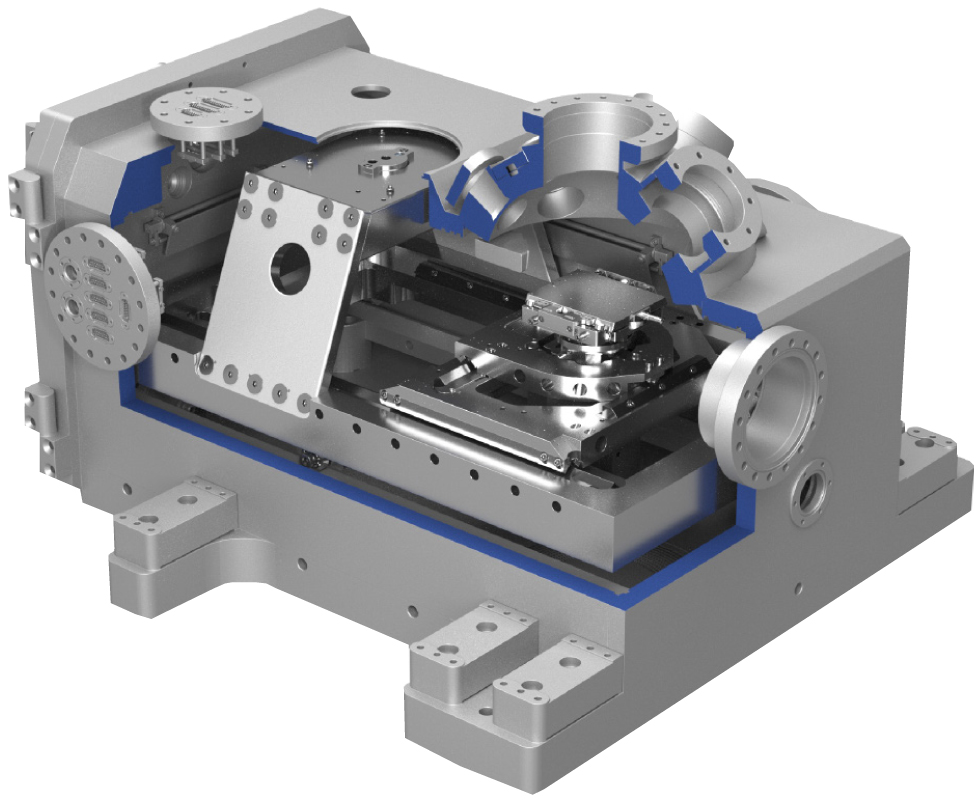
Through the combination of these two techniques true in situ three-dimensional chemical imaging becomes possible. The M6 Plus platform combines the high-end performance of the M6 with the possibility to perform in situ SPM measurements. The large area SPM unit has a scan range of up to 80 x 80 x 10 µm3 and is ideally suited to provide topographic information for true 3D SIMS measurements.
1
Powerful tool for nano characterisation
2
All standard SPM modes e.g. AFM, KPFM, multi-frequency
3
Large SPM scan range of 80 x 80 x 10 µm3
4
Unique surface profiler mode for large SIMS sputter crater measurements
5
Full compatibility with all M6 options
Micrometre position accuracy
The piezo sample stage of the M6 Plus with sub-micron position accuracy ensures fast and precise movement between the TOF-SIMS and the SPM measurement position.
The stage has a 10 nm encoder resolution and travel speeds of up to 10 mm/s which guarantees a high level of precision and stability.
True 3D chemical imaging
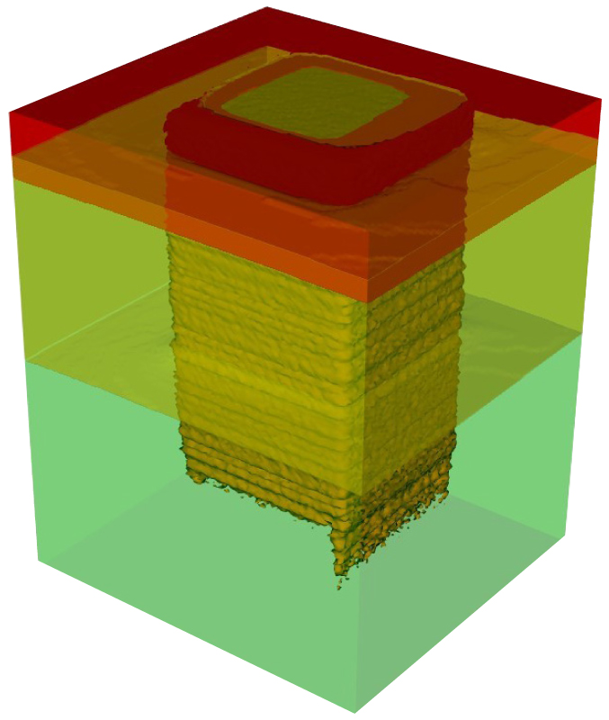
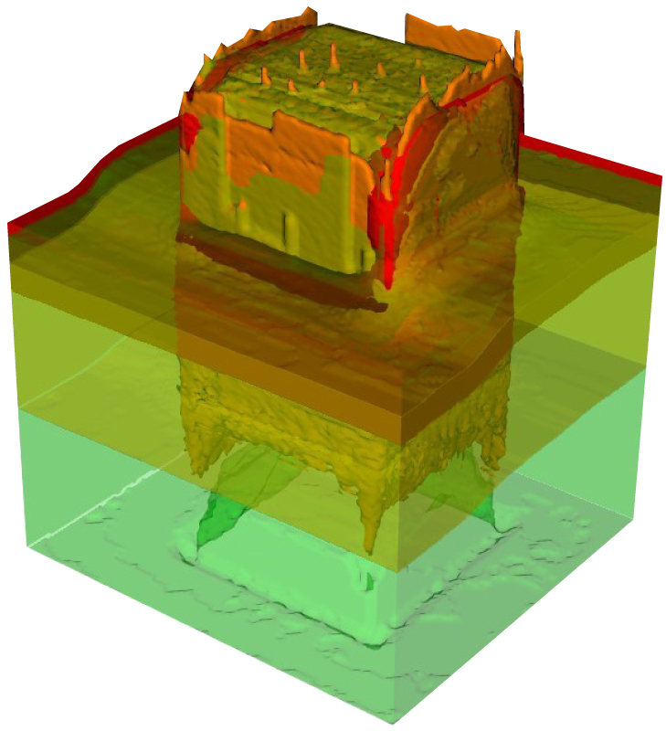
The example below shows a three-dimensional analysis of a germanium structure inside a silicon matrix. The structure has a strong initial surface topography which leads to an incorrect representation of the chemical composition if TOF-SIMS data are used alone. By combining the chemical information of TOF-SIMS with the dimensional information of SPM a true three-dimensional chemical image can be generated.
3D overlay without topography correction: SiN (red), Ge (orange), SiO2 (yellow) and Si (green).Field of view: 25 x 25 µm2
3D overlay with topography correction: SiN (red), Ge (orange), SiO2 (yellow) and Si (green). Field of view: 25 x 25 µm2
Surface profiler mode
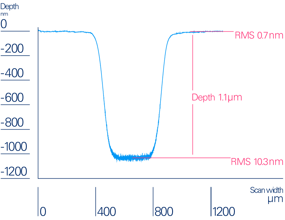
The SPM module of the M6 Plus also allows for detailed analysis of large sputter craters. In the so-called surface profiler mode multiple SPM scans are stitched together to measure long SPM line scans. This unique SPM mode is extremely valuable to precisely determine the depth of sputter craters or to measure crater roughness on the nanometer scale.
The example shows a SPM surface profiler scan of a 1.1 µm deep sputter crater in silicon. The line scan consists of multiple individual SPM scans. The recording time for the entire scan was less than 3 minutes and revealed a surface roughness of 0.7 nm (RMS) outside and 10.3 nm (RMS) inside the crater.